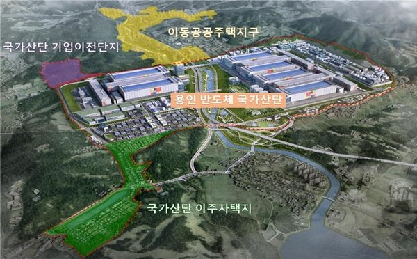
The South Korean government has moved up the beginning of construction of what is set to be the world’s largest semiconductor hub, the Yongin Semiconductor National Industrial Complex, to start in December 2026.
As part of the planning process, the country’s Ministry of Land, Infrastructure and Transport has designated the cluster as a national industrial complex three months ahead of schedule and has expedited regulatory approvals to facilitate construction commencement years ahead of schedule. Under the revised schedule, the first semiconductor plant is planned to be operational at the complex in 2030.
The Yongin Semiconductor National Industrial Complex, when complete, will span 7.28 million square meters (78.4 million square feet) and is projected to attract up to 360 trillion won ($246.4 billion) in private investments from major industry players, including Samsung Electronics Co. Ltd. and SK hynix Inc., as well as over 60 small and medium-sized suppliers specializing in materials, parts and equipment. The facility will feature six large-scale semiconductor fabrication plants, three power plants and a residential town accommodating 16,000 households, along with parks and essential facilities to support the workforce.
According to the Maeil Business Newspaper, when complete, the complex is expected to employ 1.6 million people and will generate 700 trillion won ($477.4 billion) in production inducement.
Plans to construct the complex first emerged in January, when it was reported that Samsung and SK hynix were planning to spend the equivalent of $471 million to establish a new chip hub. Reports at the time suggested that Samsung and SK hynix were planning on building 13 new fabs that would be capable of producing 7.7 million silicon wafers’ worth of semiconductors per month by 2030, or 92.4 million annually.
Notably, the current model for the Yongin Semiconductor National Industrial Complex has six fabs compared to the previously mentioned plan to build 13. How this affects capacity is not clear – the six fabs could simply be bigger in footprint and produce more than the originally proposed 13.
The complex is ultimately about putting South Korea and its leading companies in a strong position in an increasingly competitive marketplace that is also hungry for cutting-edge chips.
In a speech at the ceremony held to make the announcement, Kim Yong-kwan, president of Samsung Electronics DS Business Strategy, is quoted as saying that major economic powers such as the United States, China, Taiwan, Japan and the European Union, along with emerging countries like the Middle East and India, are heavily investing in their semiconductor industries and internalizing supply chains as key assets for national security.
He added that it was of critical importance to proceed with the complex as planned “to secure global competitiveness.”
Image: South Korean Ministry of Land, Infrastructure and Transport
Your vote of support is important to us and it helps us keep the content FREE.
One click below supports our mission to provide free, deep, and relevant content.
Join our community on YouTube
Join the community that includes more than 15,000 #CubeAlumni experts, including Amazon.com CEO Andy Jassy, Dell Technologies founder and CEO Michael Dell, Intel CEO Pat Gelsinger, and many more luminaries and experts.
THANK YOU


Leave a Comment