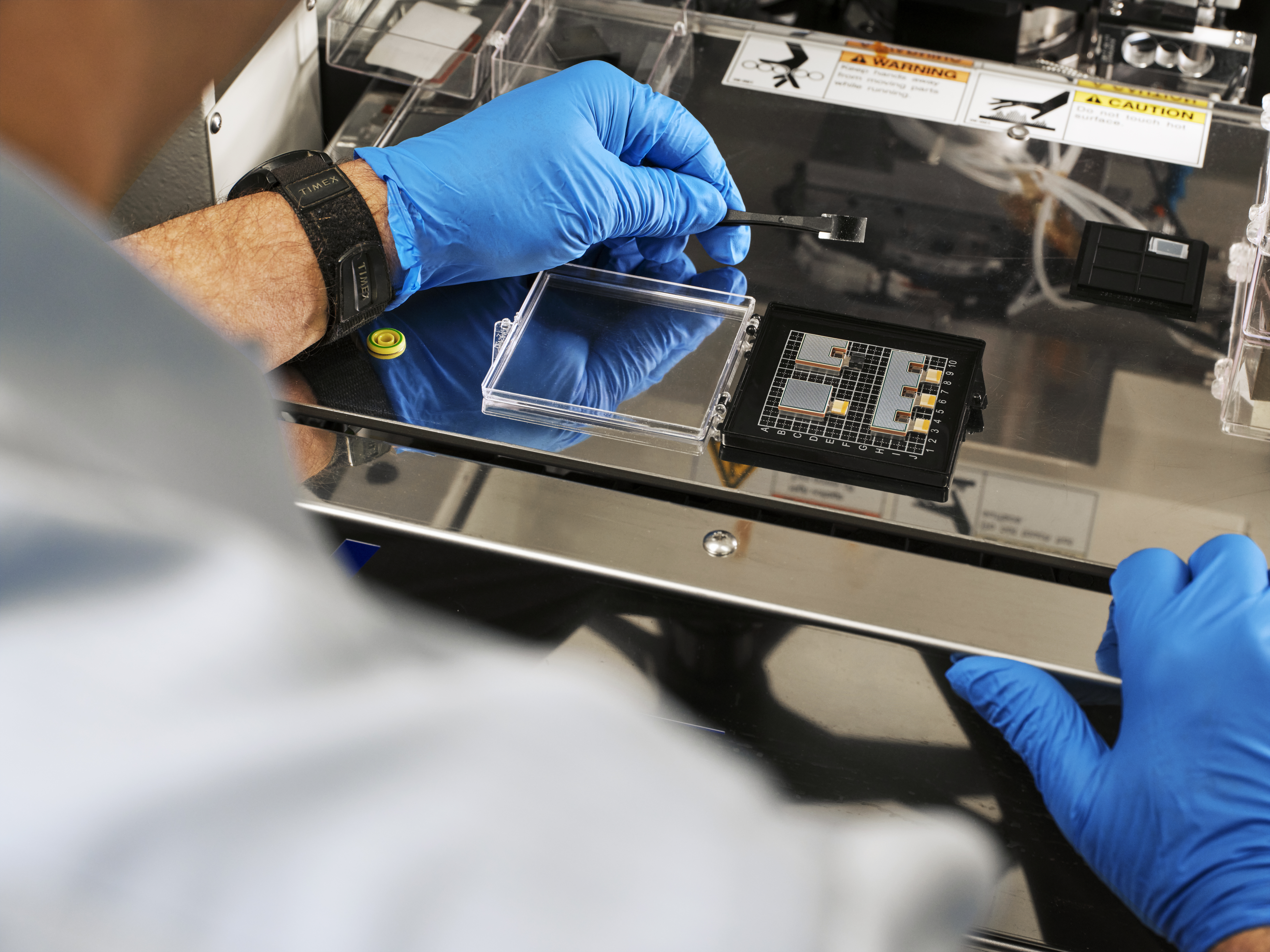
One of the ironies of graphics processing units is that, despite their high cost and limited availability, the chips spend much of their time waiting to receive instructions. A big reason, say IBM Corp. researchers, is that the connections within data centers still rely largely on copper wire instead of speedy fiber optics.
“We estimate GPUs spend about half their time idling,” said John Knickerbocker, an IBM distinguished engineer. “That’s a lot of energy being spent.”
Now, IBM says it has made significant progress in solving this problem. It’s unveiling a new process for co-packaged optics today that integrates optical components directly with electronic chips within a single package to enable connectivity between devices in a data center at the speed of light.
The company says it has built and successfully tested interconnects based upon polymer optical waveguide, a flexible and lightweight structure made from polymer materials that guides light along a path and confines light signals to minimize loss while maintaining signal integrity.
The resulting module reduces energy requirements by more than 80% compared to electrical interconnects while extending the cables that can connect components within a data center from the current one meter to hundreds of meters.
The result, IBM said, is that artificial intelligence large language models can be trained up to five times faster while saving what it estimates to be the equivalent of 5,000 U.S. homes’ annual power consumption per model trained.
Power demand surges
Before the advent of generative AI and LLMs, “demand for compute was doubling every 20 months,” said Mukesh Khare, general manager of IBM’s semiconductors division and vice president of hybrid cloud research at IBM Research. “Since LLMs have come along, it’s doubling every six months.”
Electricity consumption and its corresponding carbon footprint is one consequence of AI that is often swept under the carpet. The International Energy Agency estimated earlier this year that power use by data centers processing AI and cryptocurrency workloads could double by 2026. By that time, it will equal Japan’s total electricity consumption.
Polymer optical waveguide technology is widely used in telecommunications, data communications and sensing applications but has never been economically practical within data centers. The reasons include high initial cost, media fragility, the dominance of copper wire in legacy systems and the size of optical fibers.
At about 250 microns in diameter, or three times the width of a human hair, they take up about one-quarter of a millimeter of space. That’s significantly more than the corresponding space requirements of electronic circuits.
“While the industry had made significant progress in building faster and faster chips, the speed with which these chips can talk to each other hasn’t kept up,” Khare said. “There is a gap of several orders of magnitude.”
IBM researchers used PWG technology to line up high-density bundles of optical fibers at the edge of a chip to enable it to communicate directly through the polymer fibers. The approach achieved a half-micron or less tolerances between a fiber and the connector, which is considered the benchmark for success.
The company said its new optical structures enable chipmakers to pack six times as many optical fibers as is now possible at the edge of a silicon photonics chip. Each fiber can span just a few centimeters and carry terabits of data per second. When configured to transmit multiple wavelengths per optical channel, the CPO technology can boost bandwidth between chips as much as 80-fold.
IBM said its process has achieved an 80% size reduction from conventional optical channels and testing indicates further reductions are possible, yielding up to a 1,200% increase in bandwidth.
The co-packaged optics modules are ready for commercial use and will be manufactured at IBM’s facility in Bromont, Quebec.
Photo: IBM
Your vote of support is important to us and it helps us keep the content FREE.
One click below supports our mission to provide free, deep, and relevant content.
Join our community on YouTube
Join the community that includes more than 15,000 #CubeAlumni experts, including Amazon.com CEO Andy Jassy, Dell Technologies founder and CEO Michael Dell, Intel CEO Pat Gelsinger, and many more luminaries and experts.
THANK YOU


Leave a Comment