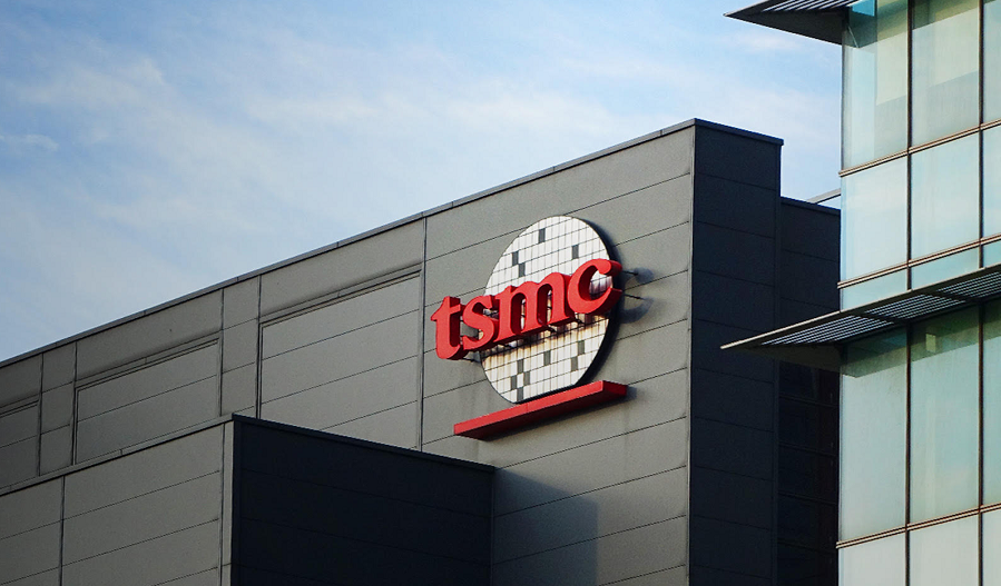
Taiwan Semiconductor Manufacturing Co. has begun mass producing chips at its new fab in Kumamoto Prefecture, Japan.
News agency Kyodo News Plus reported the milestone today.
TSMC, the world’s largest contract chipmaker, launched a semiconductor manufacturing business called JASM Inc. in Japan three years ago. It’s a joint venture with Sony Group Corp. and Denso Corp., a major auto parts supplier. TSMC broke ground on the Kumamoto fab in April 2022 and completed construction earlier this year.
The facility has more than 480,000 square feet of clean space, or space suitable for hosting chipmaking equipment. It makes logic chips based on manufacturing processes in the 28-nanometer to 12-nanometer range. Those technologies are several generations behind TSMC’s newest three-nanometer node, but they’re still widely-used to make circuits that prioritize cost-efficiency over maximizing performance.
The new fab’s first customers include Sony and Denso, the companies with which TSMC launched its JASM joint venture. The plant will make camera chips for Sony, as well as processors optimized to power vehicle subsystems.
Car chips, particularly those that support sensitive components such as brakes, must adhere to stricter reliability standards than other circuits. Many use a technique known as lockstep processing to reduce the risk of errors. In lockstep mode, every single computation is performed by at least two different cores and the results are compared afterwards to identify inconsistencies.
Many car processors feature a system-on-chip design that combines a central processing unit with other components. In some cases, one of those components is a network accelerator optimized to coordinate the flow of data between a vehicle’s subsystems. Some car processors also include cybersecurity and artificial intelligence modules.
In March, TSMC plans to start building a second fab next to its new Kumamoto facility. The upcoming plant is expected to come online by the end of 2027. It will be capable of making chips using six-nanometer and seven-nanometer processes, which are not supported by the existing fab.
Once both plants are fully operational, they will have enough capacity to produce 100,000 12-inch wafers per month. TSMC estimates that construction will cost $20 billion to complete. The Japanese government is providing billions of dollars in subsidiaries to support the project.
It’s believed TSMC could further expand its manufacturing operations in Japan down the road. Earlier this year, CNBC reported that the company was weighing the possibility of building an advanced chip packaging plant in the country. Advanced chip packaging is the technology that makes it possible to link together multiple silicon dies into a single processor.
It’s believed TSMC might use the facility to make CoWoS hardware. This is a type of packaging technology that is used in, among other products, Nvidia Corp.’s data center graphics cards. TSMC has maintained an advanced packaging research and development hub in Japan since 2021.
Photo: TSMC
Your vote of support is important to us and it helps us keep the content FREE.
One click below supports our mission to provide free, deep, and relevant content.
Join our community on YouTube
Join the community that includes more than 15,000 #CubeAlumni experts, including Amazon.com CEO Andy Jassy, Dell Technologies founder and CEO Michael Dell, Intel CEO Pat Gelsinger, and many more luminaries and experts.
THANK YOU


Leave a Comment